Electronics 3 Oz Copper Base Multilayer PCB , Rigid Custom Made Pcb Boards Security
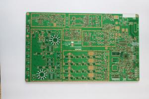
8-Layer Electronics 3 Oz Copper Base Multilayer Rigid PCB Security Electronics PCB
Key Specifications/Special Features:
Key Specifications
Number of layers: 8L
Base-material: FR4, TG150
Thickness: 1.8 mm+/-10%
Final-Cu: 35um
Impedance: No
Blind and buried via: Yes
Min. Drill hole: 0.25mm
Min. Line space: 0.127mm
Min. Line width: 0.127mm
Mech. treatment: Routing
Surface treatment: ENIG
Solder-mask: Green
Legend-Print: white
100% E-test: Yes
Reasonable price and professional services.
UL,SGS,ISO9001,ISO14001,RoHS and ISO TS16949
Main Export Markets:
Asia
Australasia
Central/South America
Eastern Europe
Mid East/Africa
North America
Western Europe
Specification:
8-Layer Electronics 3 Oz Copper Base Multilayer Rigid PCB Security Electronics PCB
Green Soldermask White Silkscreen,
FR - 4 epoxy glass fiber cloth substrate, based on epoxy resin as binder,
with electronic level glass fiber cloth as reinforcing material of substrate.
Its bonding sheet and thin copper-clad r.p. panel and inner core is an important base material
in production of multilayer printed circuit board,
This kind of product is mainly used for double-sided PCB, dosage is very large.
Epoxy glass fiber cloth substrate, the most widely used model for FR - 4,
in recent years because of the electronic product installation technology
and PCB technology development needs, appeared high Tg FR - 4 products.
Specification:
8-Layer Electronics 3 Oz Copper Base Multilayer Rigid PCB Security Electronics PCB,
FR - 4 epoxy glass fiber cloth substrate, based on epoxy resin as binder, with electronic level glass fiber cloth as reinforcing material of substrate. Its bonding sheet and thin copper-clad r.p. panel and inner core is an important base material in production of multilayer printed circuit board,This kind of product is mainly used for double-sided PCB, dosage is very large. Epoxy glass fiber cloth substrate, the most widely used model for FR - 4, in recent years because of the electronic product installation technology and PCB technology development needs, appeared high Tg FR - 4 products.
Immersion Gold and the difference between gold-plated plate 1, immersion gold and gold-plated crystal structure is not the same as the thickness of gold for gold than gold-plated lot of gold will be gold-plated gold is more yellow, more satisfied customers. 2, immersion gold and gold-plated crystal structure is not the same, Shen Jin is easier than gold-plated welding, will not cause poor welding, causing customer complaints. Immersion gold plate of the stress more easily controlled, there is a bonding of products, more conducive to the processing of bonding. But also because of the gold than the gold-plated soft, so Shen Jin-board do not wear gold finger. 3, immersion gold plate only nickel gold pads, skin effect of the signal transmission is in the copper layer will not affect the signal. 4, immersion gold than gold-plated crystal structure is more compact, not easy to produce oxidation. 5, with the wiring more and more dense, line width, spacing has come to 3-4MIL. Gold is easy to produce gold short-circuit. Immersion gold plate only nickel gold on the pad, it will not produce gold short-circuit. 6, immersion gold plate only nickel gold on the pad, so the resistance of the line with the combination of copper layer is more solid. Engineering will not compensate for the spacing of the impact. 7, generally used for the relatively high requirements of the board, flatness is better, generally use immersion gold, immersion gold generally do not appear after the assembly of the black pad phenomenon. Immersion gold plate flatness and standby life as good as gold-plated plate
Parameter:
| o |
Item |
Data |
| 1 |
Layer: |
1 to 24 layers |
| 2 |
Material type: |
FR-4, CEM-1, CEM-3, High TG, FR4 Halogen Free, Rogers |
| 3 |
Board thickness: |
0.20mm to 3.4mm |
| 4 |
Copper thickness: |
0.5 OZ to 4 OZ |
| 5 |
Copper thickness in hole: |
>25.0 um (>1mil) |
| 6 |
Max. Board Size: |
(580mm×1200mm) |
| 7 |
Min. Drilled Hole Size: |
4mil(0.1mm) |
| 8 |
Min. Line Width: |
3mil (0.075mm) |
| 9 |
Min. Line Spacing: |
3mil (0.075mm) |
| 10 |
Surface finishing: |
HASL / HASL lead free, HAL, Chemical tin, Chemical Gold, Immersion Silver/Gold, OSP, Gold plating |
| 11 |
Solder Mask Color: |
Green/Yellow/Black/White/Red/Blue |
| 12 |
Shape tolerance: |
±0.13 |
| 13 |
Hole tolerance: |
PTH: ±0.076 NPTH: ±0.05 |
| 14 |
Package: |
Inner packing: Vacuum packing / Plastic bag,Outer packing: Standard carton packing |
| 15 |
Certificate: |
UL,SGS,ISO 9001:2008 |
| 16 |
Special requirements: |
Buried and blind vias+controlled impedance +BGA |
| 17 |
Profiling: |
Punching, Routing, V-CUT, Beveling |
Place of Origin: |
Guangdong China (Mainland) |
Brand Name: |
XCE |
Model Number: |
XCEPCB008 |
Base Material: |
FR4 |
Copper Thickness: |
0.3-3oz |
Board Thickness: |
0.3-6mm |
Min. Hole Size: |
0.2mm |
Min. Line Width: |
3mil |
Min. Line Spacing: |
3mil |
Surface Finishing: |
HASL, OSP, Immersion Gold/Au, Immersion silver, etc. |
Solder mask: |
Green |
PCB Standard: |
IPC-A-610 E Class II-III |
Wrap and twist: |
5% |
Layer Count: |
1-22 |
profiling punching: |
Routing, V-CUT, Beveling |
Max board size: |
1200mm*600mm |
Hole tolerance: |
PTH:±0.075,NTPH:±0.05 |
PCB Tolerance of finished thickness: |
±5% |
PCB: |
Customized |
Product name: |
pcb
|
Product Tags:

|
|
Electronics 3 Oz Copper Base Multilayer PCB , Rigid Custom Made Pcb Boards Security Images
|